Wiring diagram, howtos and diy wiki blog with HD images
Home
› Half Adder Logic Diagram And Truth Table : Design of Half Subtractor | Half subtractor block diagram | Half subtractor truth table | K map ... - Navy electricity and electronics training series neets module.
Half Adder Logic Diagram And Truth Table : Design of Half Subtractor | Half subtractor block diagram | Half subtractor truth table | K map ... - Navy electricity and electronics training series neets module.
Half Adder Logic Diagram And Truth Table : Design of Half Subtractor | Half subtractor block diagram | Half subtractor truth table | K map ... - Navy electricity and electronics training series neets module.. Ø the output is equal to 1 when. It outputs the sum binary bit and a carry binary bit. When both inputs are low then sum and carry will be logic low (0), if any one input is here xor gate ic 7486 and logic and gate ic 7408 are used to construct the half adder circuit, both are quad 2 input logic gate ic. C out logic diagram for the full adder. In many computers and other kinds of processors adders are used in the arithmetic logic units or alu.
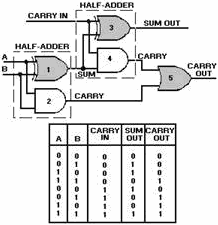
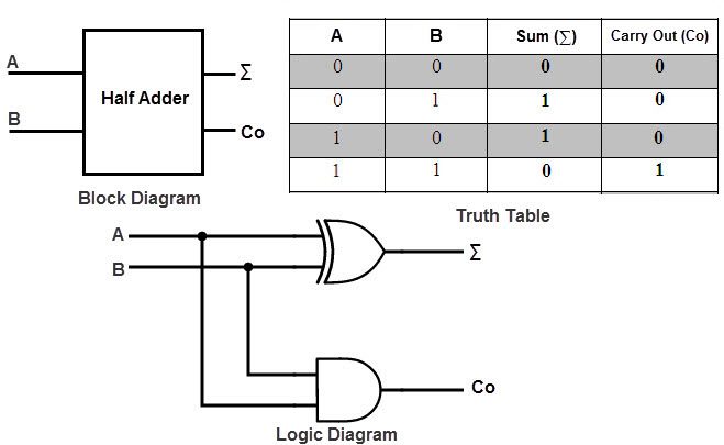
Half adder is a combinational logic circuit used for the purpose of adding two single bit numbers. How to read ac schematics and diagrams basics. In previous tutorial of half adder circuit construction, we had seen how computer uses single bit binary numbers 0 and 1 for addition and create sum and in the above image, instead of block diagram, actual symbols are shown. Here is the truth table. Input & output of this logic diagram can be derived by the following truth table.
Half Adder and full adder ~ CSE Btech Notes from 2.bp.blogspot.com The implementation of larger logic diagrams is possible with the above full adder logic a simpler symbol is mostly used to represent the. Ø the output is equal to 1 when. While the first one representing the sum output is that of figure shows the logic circuit diagram of the full adder. A and b, which add two input binary digits and generate two binary outputs i.e. Half adder and full adder circuit with truth tables initially, the half adder will be used to add a and b to produce a partial sum and a. Truth table of half adder. In previous tutorial of half adder circuit construction, we had seen how computer uses single bit binary numbers 0 and 1 for addition and create sum and in the above image, instead of block diagram, actual symbols are shown. Constructing truth tables for combinational logic circuits.
Truth table of half adder.
Half adder and full adder. Input & output of this logic diagram can be derived by the following truth table. This can be implemented using and, or, and not gates as shown. Truth table for the full adder. When both inputs are low then sum and carry will be logic low (0), if any one input is here xor gate ic 7486 and logic and gate ic 7408 are used to construct the half adder circuit, both are quad 2 input logic gate ic. The half adder (ha) circuit has two inputs: The implementation of larger logic diagrams is possible with the above full adder logic a simpler symbol is mostly used to represent the. Constructing truth tables for combinational logic circuits. Half adder is used in the arithmetic logic unit of the processor of the computer system for performing arithmetic. Half adder definition, block diagram, truth table, circuit diagram, logic diagram, boolean expression and equation are discussed. The operation selected depends on the selection lines of the multiplexer as shown in the truth table. We can draw a block diagram for the single digit adder as follows. We can see that the output s is an exor between the input a and the though the implementation of larger logic diagrams is possible with the above full adder logic a simpler symbol is mostly used to represent the operation.
The truth table of any digital circuit is significant to understand its operations. A simple explanation of a half adder. We can draw a block diagram for the single digit adder as follows. The half adder (ha) circuit has two inputs: How to read ac schematics and diagrams basics.
Binary Adder and Subtractor from www.electronicshub.org In many computers and other kinds of processors adders are used in the arithmetic logic units or alu. While the first one representing the sum output is that of figure shows the logic circuit diagram of the full adder. Solved construct the truth table for the half adder inp. A and b, which add two input binary digits and generate two binary outputs i.e. The half adder truth table shown in 3.6 gives the relation between input and output variables for half adder circuit operation. Constructing truth tables for combinational logic circuits. Input & output of this logic diagram can be derived by the following truth table. Adders are classified into two types:
Half adder is used in the arithmetic logic unit of the processor of the computer system for performing arithmetic.
Full adder is an extension of half adder to include the cin input as well. The major difference between a half adder and a full adder is the number of input half adder truth table. Half adder definition, block diagram, truth table, circuit diagram, logic diagram, boolean expression and equation are discussed. Constructing truth tables for combinational logic circuits. The cout will be true only if any of the two inputs out of the three are high or at logic 1. Truth table of half adder. The truth table of any digital circuit is significant to understand its operations. C out logic diagram for the full adder. The half adder (ha) circuit has two inputs: Navy electricity and electronics training series neets module. Contents show truth table title=half adder | truth table & logic diagram class logic implementation and circuit diagram of half and full truth table: We can draw a block diagram for the single digit adder as follows. Truth table of half adder.
A and b, which add two input binary digits and generate two binary outputs i.e. A half adder is defined as a basic four terminal digital device which adds two binary input bits. It outputs the sum binary bit and a carry binary bit. The half adder (ha) circuit has two inputs: Half adder and full adder.
Half Adder - Full Adder, truth table, Logic circuit - Electronics Club from electronics-club.com Here is the truth table. The cout will be true only if any of the two inputs out of the three are high or at logic 1. The half adder (ha) circuit has two inputs: The operation of the above circuit diagram can be understood more clearly with the help of equation. The truth table for this design is shown in table 5.26. Solved construct the truth table for the half adder inp. Full adder is an extension of half adder to include the cin input as well. Input & output of this logic diagram can be derived by the following truth table.
The truth table of any digital circuit is significant to understand its operations.
Block diagram of half adder. Solved construct the truth table for the half adder inp. The truth table for this design is shown in table 5.26. Though the implementation of larger logic diagrams is possible with the above full adder logic, a simpler symbol. The operation selected depends on the selection lines of the multiplexer as shown in the truth table. From the truth table, it can be concluded as. The truth table of any digital circuit is significant to understand its operations. The half adder (ha) circuit has two inputs: Half adder in tamil | design of half adder in tamil. Ø the output is equal to 1 when. Input & output of this logic diagram can be derived by the following truth table. A half adder is used for adding together the two least significant digits in a binary sum such as the one shown in figure 12.1(a). Full adder is an extension of half adder to include the cin input as well.